Chaosheng Company specializes in producing any order of HDI, high
frequency mixed pressure HDI, soft and hard combined HDI,
multi-layer ceramic, special size, mixed copper base, metal
cladding, high and low copper, buried, buried resistance, special
process, special materials High-end (PCB, FPC) circuit boards;
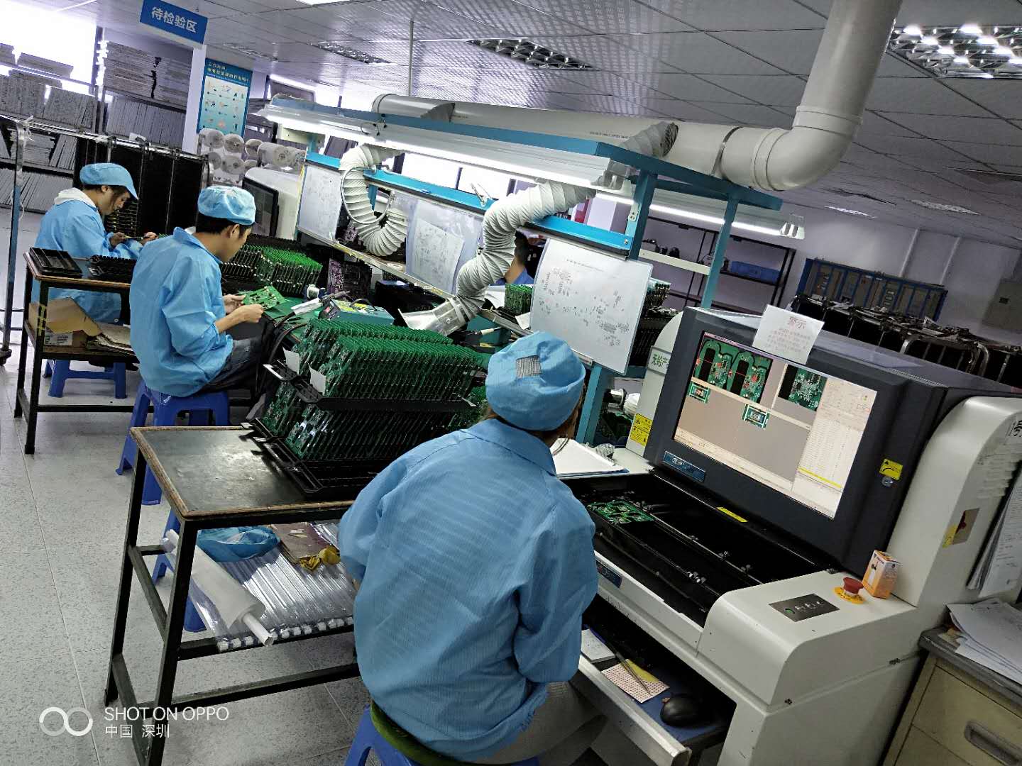
product design, product development, software development, PCBA and
FPCBA (SMT, post-weld, plug-in), processing and integrated
production plants.
Factory set up history :
1982 the Japanese factory was established;
Zhe Jiang Factory
Jiang Xi Factory 2006 Guangdong Shenzhen Division
2007 Dong Guan Factory
2010 Jiang Su, Si Chuan Factory
Chad Sheng’s business includes real estate, plastic, metals, LED, finance,
high preision PCB equipment, chemicals, high precision PCB & FPC
manufacture, More than 100 main customers are multi-national enterprise. Existing total factory area is more than 100,000 sqm. The
capacities of PCB business are as below and the total turnover is over 30 billion RMB per year.
Double sided PCB 650,000 sqm/month
2L to 80L HDI with 1 to 4 layers
blind and buried PCB
& high layer-count PCB 160,000 sqm/month
Flexible Printed Ciccuit (FPC) 150,000 sqm/month
Chao Sheng can produce different kinds of PCBs such as :2-80 layers high layer count PCB
Flexible printed circuit, double-sided & multi-layer Aluminium PCB,
ceramic PCB
1 to 4 layers blind & buried holes HDI PCB
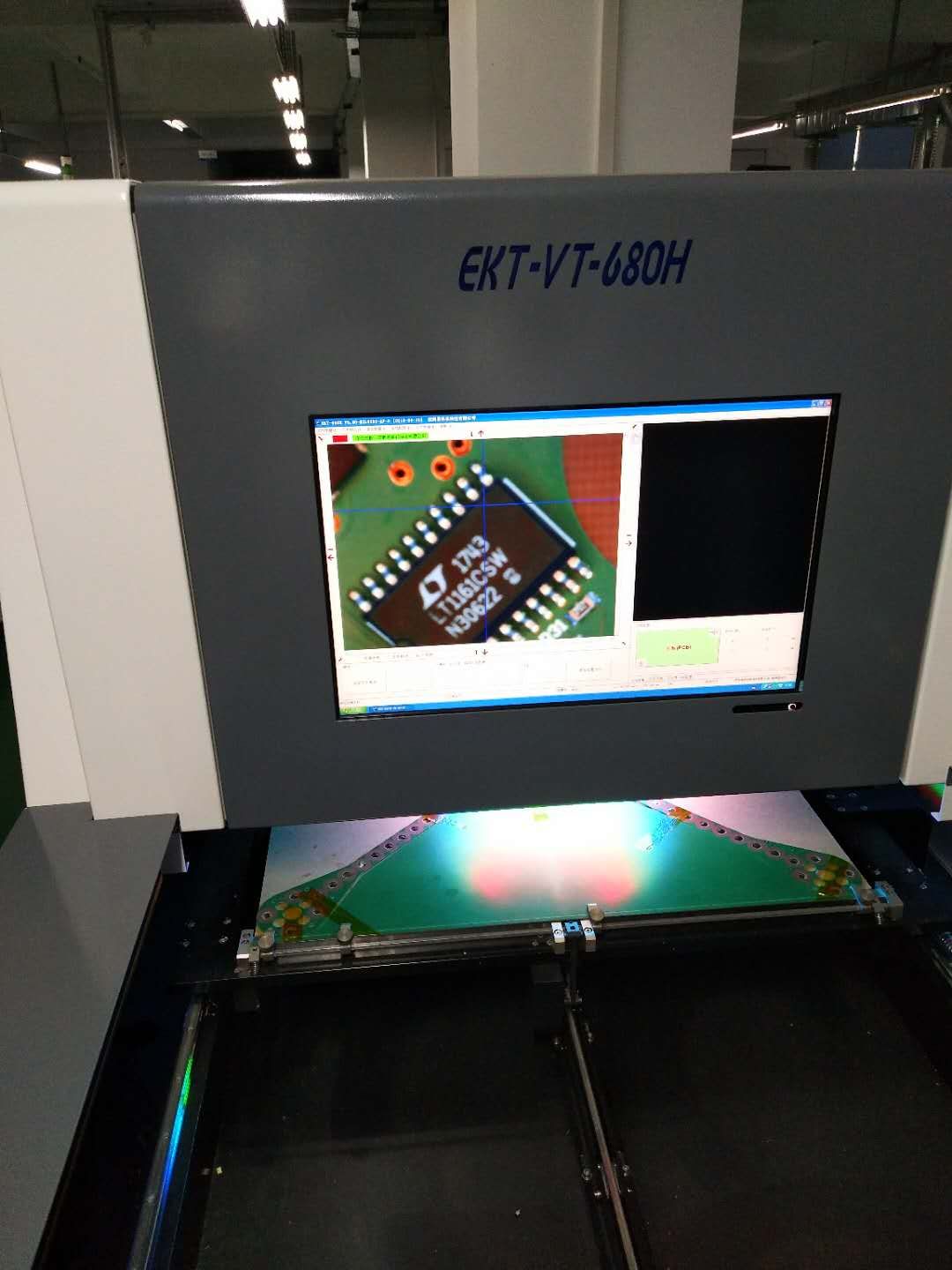
Chao Sheng has Japan PCB & got the international certification such as UL, ISO9000, TS16949, ISO14000 AND QS8000. By
use of modern technologies, IE, ERP and contemporary quality
management systems and equipped with imported advanced precision
equipments and production lines, Company’s objective “Global resources →Japan technology→create world class number one” can be achieved.
Our main customers are ABB, Omron, Seoul, Hua Wei, Ericsson,
Toyota, Apple, Sony, Alco, BOE, Tongli, San Sheng, Samsung, LG,
Fiber Home prod & after sales service, Emerson, etc. Many foreign
and domestic famous enterprises build up their own brand name in
the past years and have very good reputation. In order to fulfill
customer’s step, Chao Sheng provides high end, middle end and low end
products and services to customers. Our business philosophy - “better, faster and cost effective” are agreed by customers.
Company continues to concern environmental protection and clean
production. We insist on continue developing strategy and stick on
China and Global environmental convention. We have perfect
environmental protection system and facilities which can treat
waste, reduce waste and reduce energy. Company already achieved
Guang Dong Province’s clean production requirement and exceed China (class 1) clean production requirement.
Base on our mission “To provide high quality PCB, on time and satisfactory services to the global electronic industry” and core system value “trust, mutual help, improvement, share customers are the core,
markets are the trend” , Chao Sheng must achieve “to grow up to be first class PCB enterprise, and create value to
customers, employees, society & share holers.”
Our goal is quality first, on time delivery, continuous improvement,
customer satisfaction and provide first class services. We welcome
all customers to visit our plants to give valuable comments, and
hope to build up a long-term cooperation relationship.